July 1, 2025 marks a significant milestone in materials science with the discovery of materials exhibiting intrinsic p-type and n-type duality (DDCP). This novel property enables a single crystalline material to conduct both electrons (n-type) and holes (p-type) depending on crystallographic direction, opening transformative possibilities for semiconductors, thermoelectrics, and green technology aligned with India’s Make in India vision.
Novel DDCP Phenomenon and Mechanism
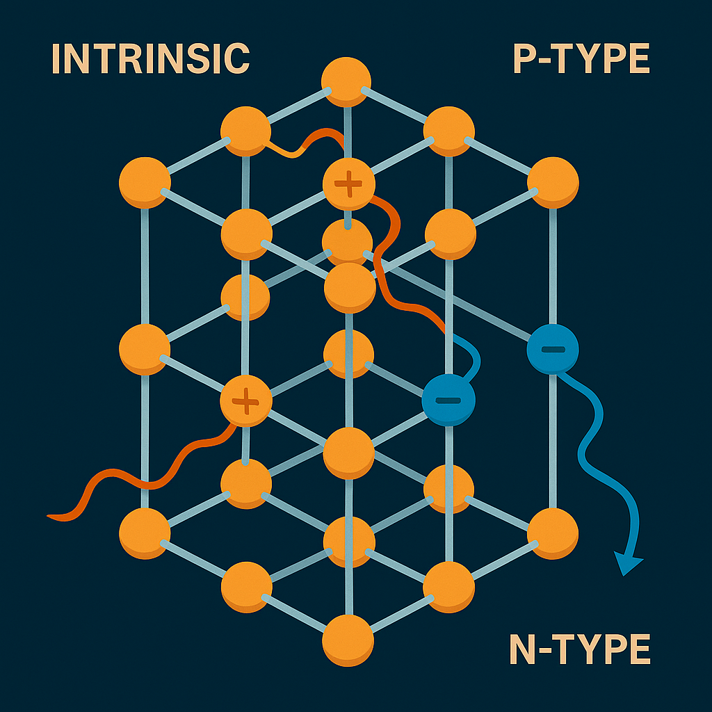
Materials with Direction-Dependent Charge Polarity (DDCP) possess crystallographic asymmetry that assigns opposite majority carriers along different axes. For example, in certain CrSb single crystals, one crystallographic axis favors electron conduction (n-type), while the perpendicular axis favors hole conduction (p-type)1. This duality arises from intrinsic variations in the local electronic band structure, where the valence and conduction band edges shift relative to the Fermi level across directions.
Visualization of intrinsic p/n-type duality in novel DDCP material
Implications for Semiconductor Devices
- Simplified Device Architectures
Conventional p–n junctions require doping and heterostructure fabrication. DDCP materials can form junctions within a single crystal, reducing fabrication complexity, defect density, and costs. - Enhanced Performance
- Reduced Interface Losses: Eliminates grain‐boundary scattering and interface traps common in doped junctions.
- Compact Integration: Enables ultra‐thin, monolithic diodes, transistors, and logic gates within one wafer, enhancing device scaling.
Advances in Thermoelectric Materials
The thermoelectric efficiency of a material is gauged by its dimensionless figure of merit ZT=S2σTκZT=κS2σT. DDCP materials can optimize:
- Seebeck coefficient (SS) by aligning charge polarity with thermal gradients.
- Electrical conductivity (σσ) directionally for maximal power factor.
- Thermal conductivity (κκ) via anisotropic phonon scattering.
This directional control could yield ZT values exceeding current records, enabling efficient electricity generation from waste heat in industrial and automotive sectors1.
Alignment with ‘Make in India’ and Green Technology
- Indigenous R&D: Strengthens India’s materials innovation ecosystem by fostering in‐country development of DDCP materials.
- Cost-Effective Manufacturing: Single‐crystal growth and direction‐controlled processes reduce reliance on complex heterostructure photolithography.
- Sustainable Energy: Thermoelectric applications support waste‐heat recovery, reducing carbon emissions and enhancing energy efficiency.
Future Directions and Challenges
- Scalability: Industrial synthesis of high‐quality DDCP single crystals (e.g., CrSb) requires process optimization.
- Device Integration: Engineering directional contacts and designing circuits that leverage anisotropic conduction.
- Stability Testing: Long‐term performance under thermal cycling, humidity, and operational stress must be validated.
This discovery of intrinsic p/n-type duality heralds a new era in semiconductor and thermoelectric technologies, promising simplified fabrication, enhanced performance, and alignment with India’s strategic goals in indigenous innovation and green energy